About Us
Over 20 years dedicated to solar PV, delivering high-quality photovoltaic solutions to customers worldwide.
JOYOSOLAR
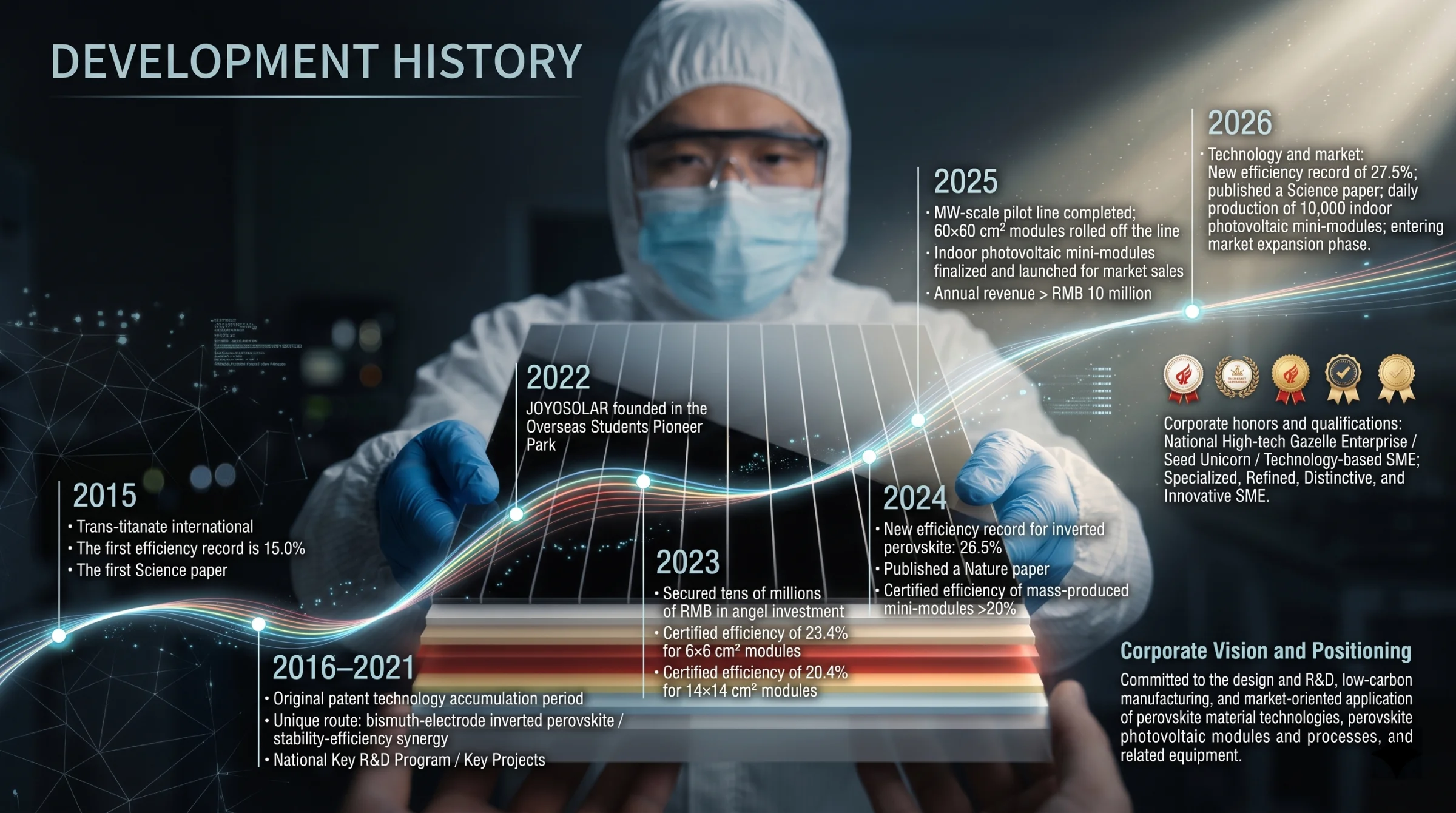
JOYOSOLAR was founded in 2022 at the Wuhan Overseas Students Entrepreneurship Park. The founding team has dedicated years to perovskite photovoltaic technology, driven by the ideal of contributing to the nation through academia. The company is committed to the design and development of perovskite material technology, perovskite photovoltaic modules and processes, related equipment, low-carbon manufacturing, and market-oriented applications. Based on verifiable technical indicators, the company will develop phased products and actively promote the early industrialization of low-cost, high-efficiency new perovskite photovoltaic technology, providing new technical options for achieving the goals of carbon peak and carbon neutrality.

Milestones

Wuhan, China
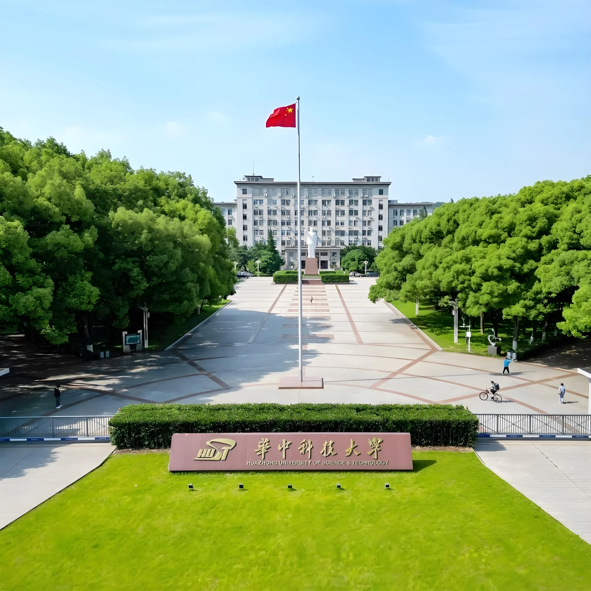
Huazhong University of Science and Technology, Wuhan, China - Chen Wei / Liu Zonghao Team

JOYOSOLAR
Founder
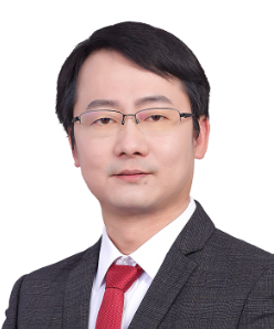
Prof. Chen Wei
Chief Scientist
B.S. and Ph.D. from Tsinghua University; postdoctoral researcher at HKUST and visiting scholar at NIMS, Japan
Recipient of the National Ten Thousand Talent Program Leading Scientist, Young Top-Notch Talent, and National Science Fund for Excellent Young Scholars
Listed among the world's top 2% of scientists with lifetime scientific impact
Author of more than 130 SCI papers in journals including Science and Nature; holder of over 30 granted patents
An early explorer, continuous innovator, and industrialization practitioner in inverted perovskite solar cells
Achieved the world's first certified efficiency record for inverted perovskite solar cells, recognized on authoritative efficiency tables
Obtained the world's first third-party stability certification report for perovskite modules issued to an academic institution
Led 8 national-level projects, including key programs under the National Key R&D Plan and NDRC open-challenge projects
Qualifications
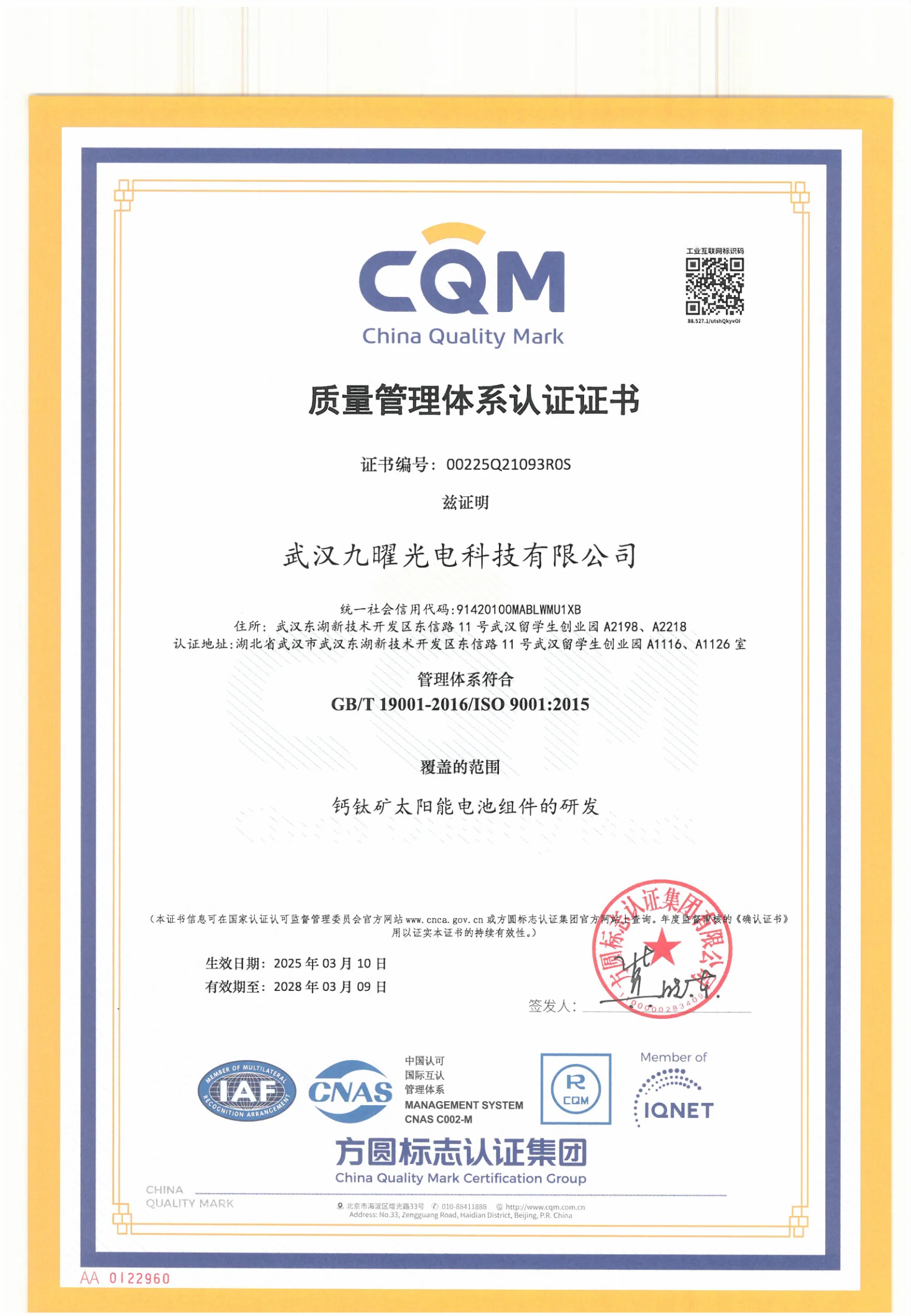
ISO 9001 Quality Management System Certification
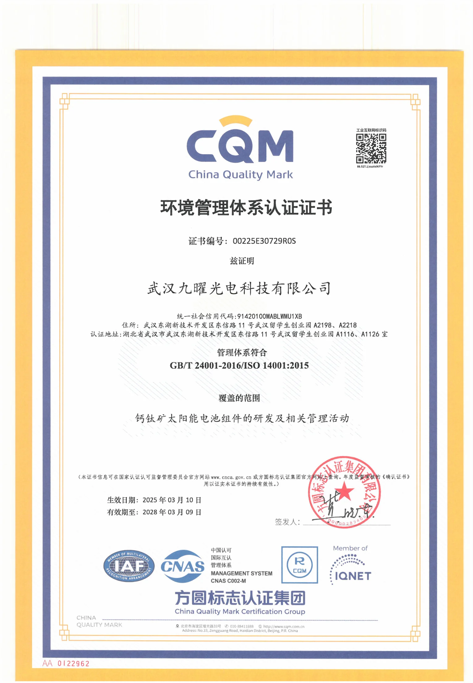
ISO 14001 Environmental Management System Certification
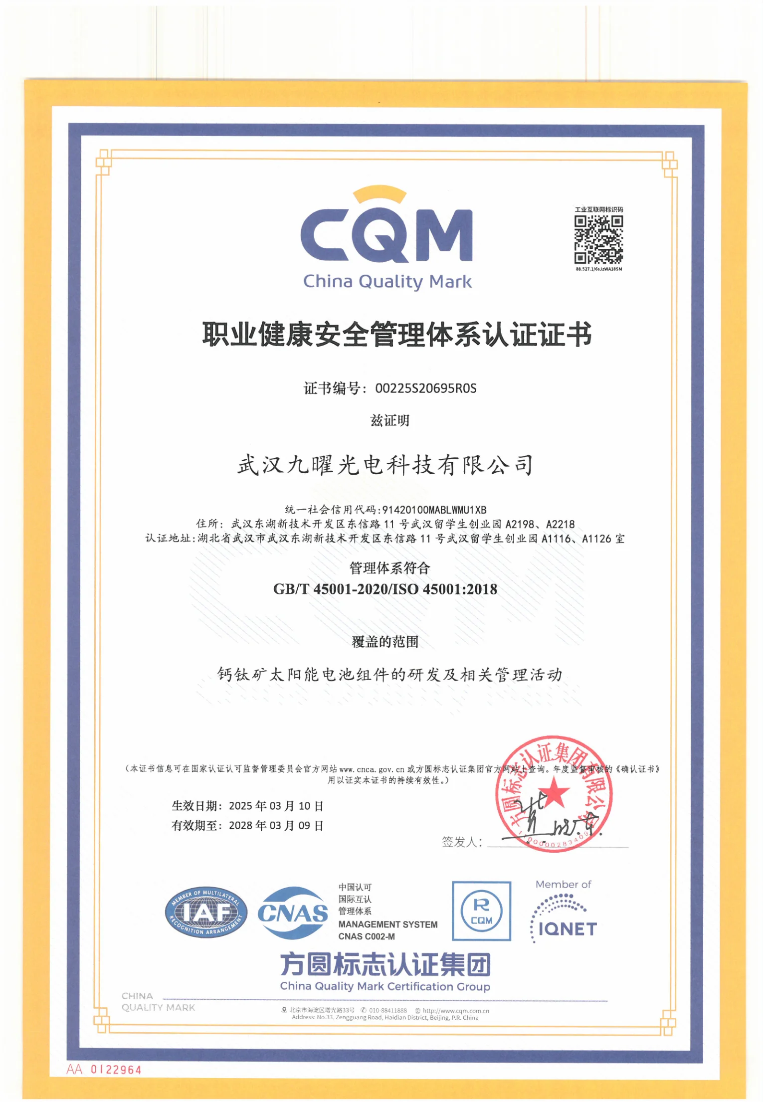
ISO 45001 Occupational Health and Safety Management System Certification
Patents
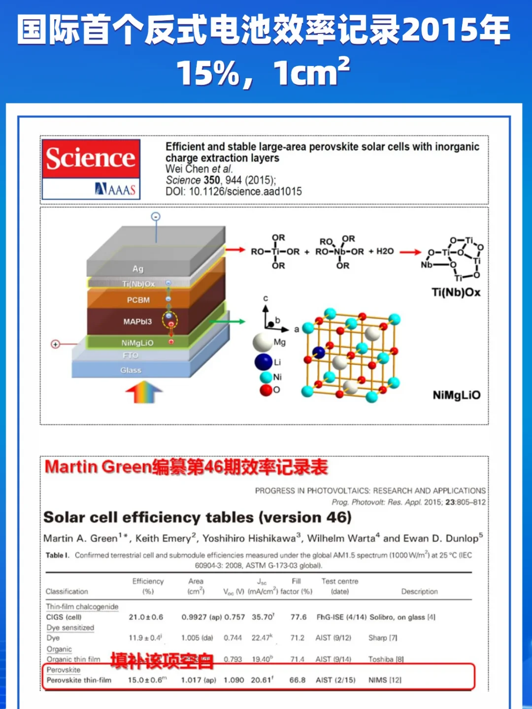
Science 15%
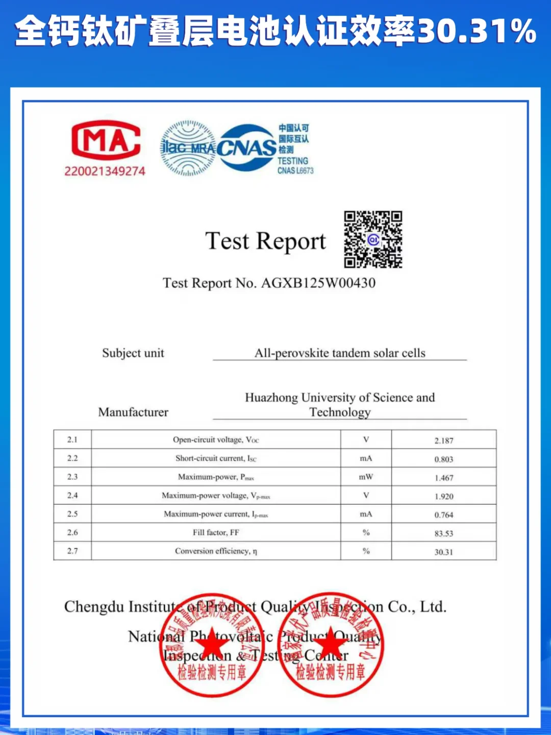
30.31%
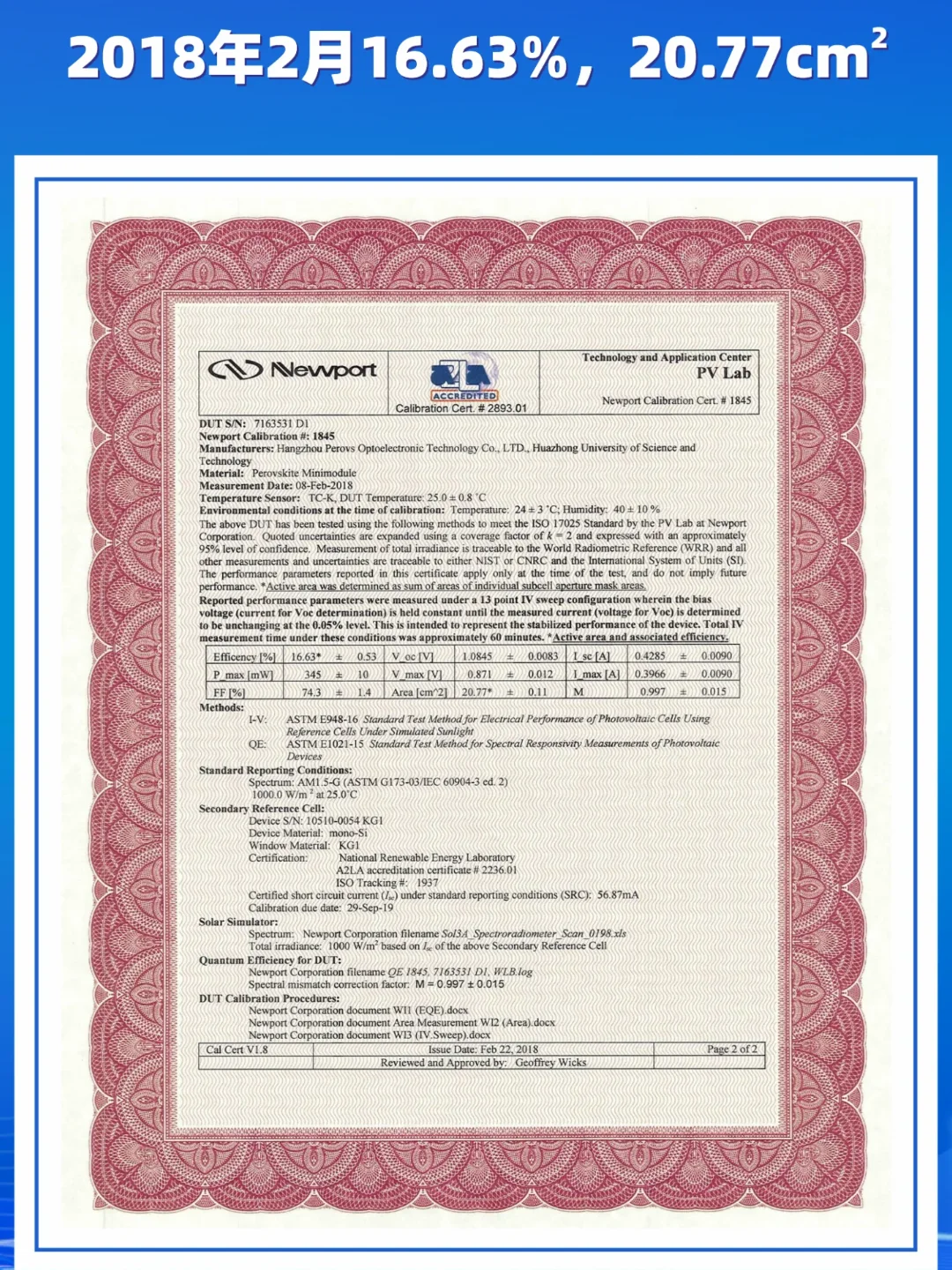
16.63%
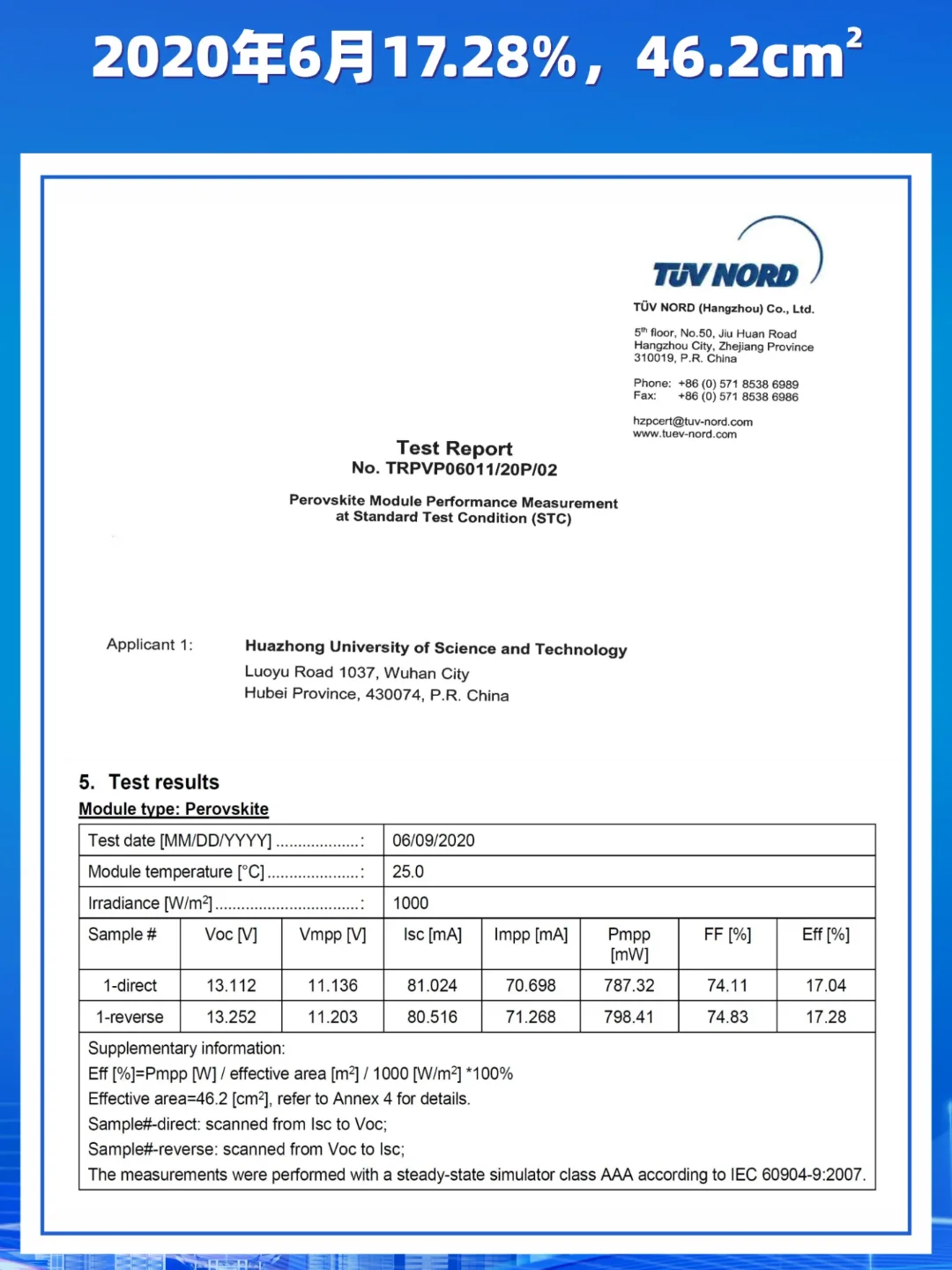
17.28%
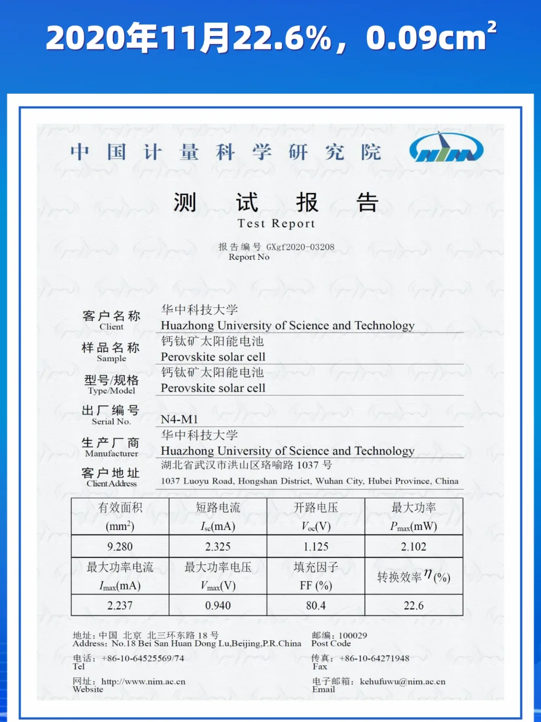
22.6%
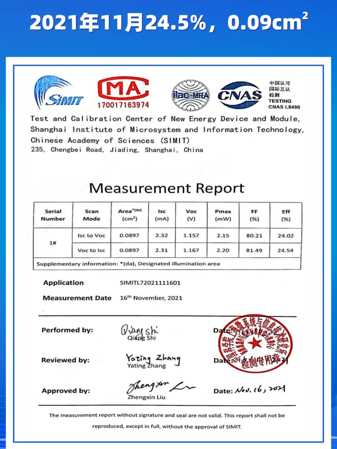
24.5%
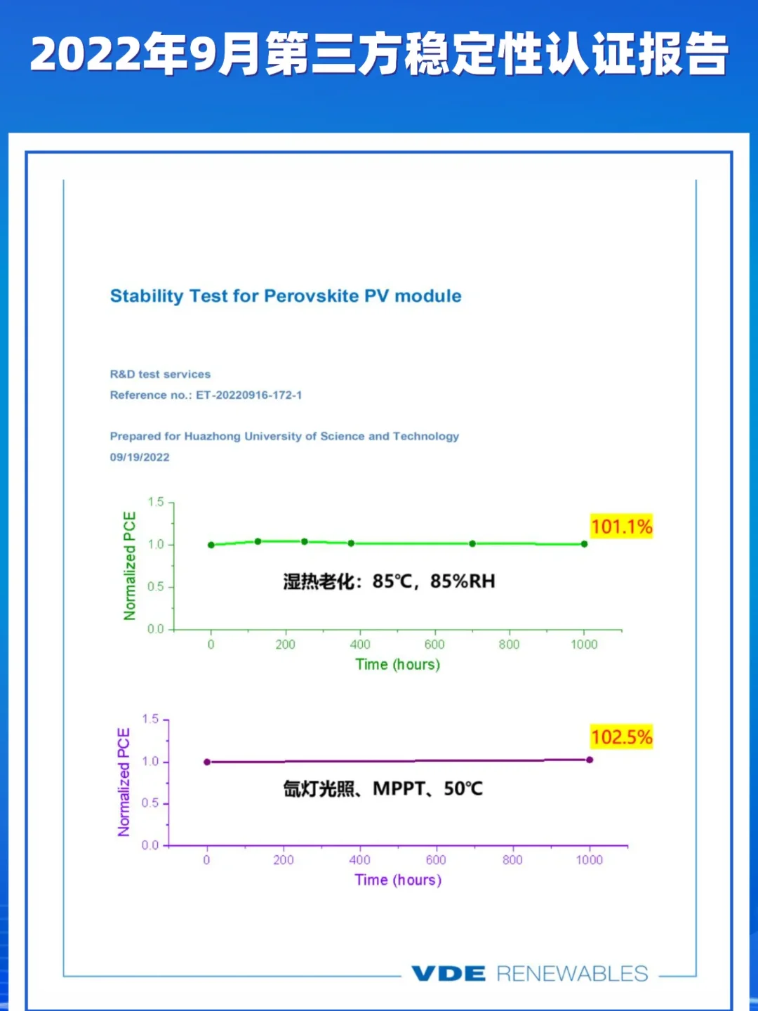
Third-Party Stability Report
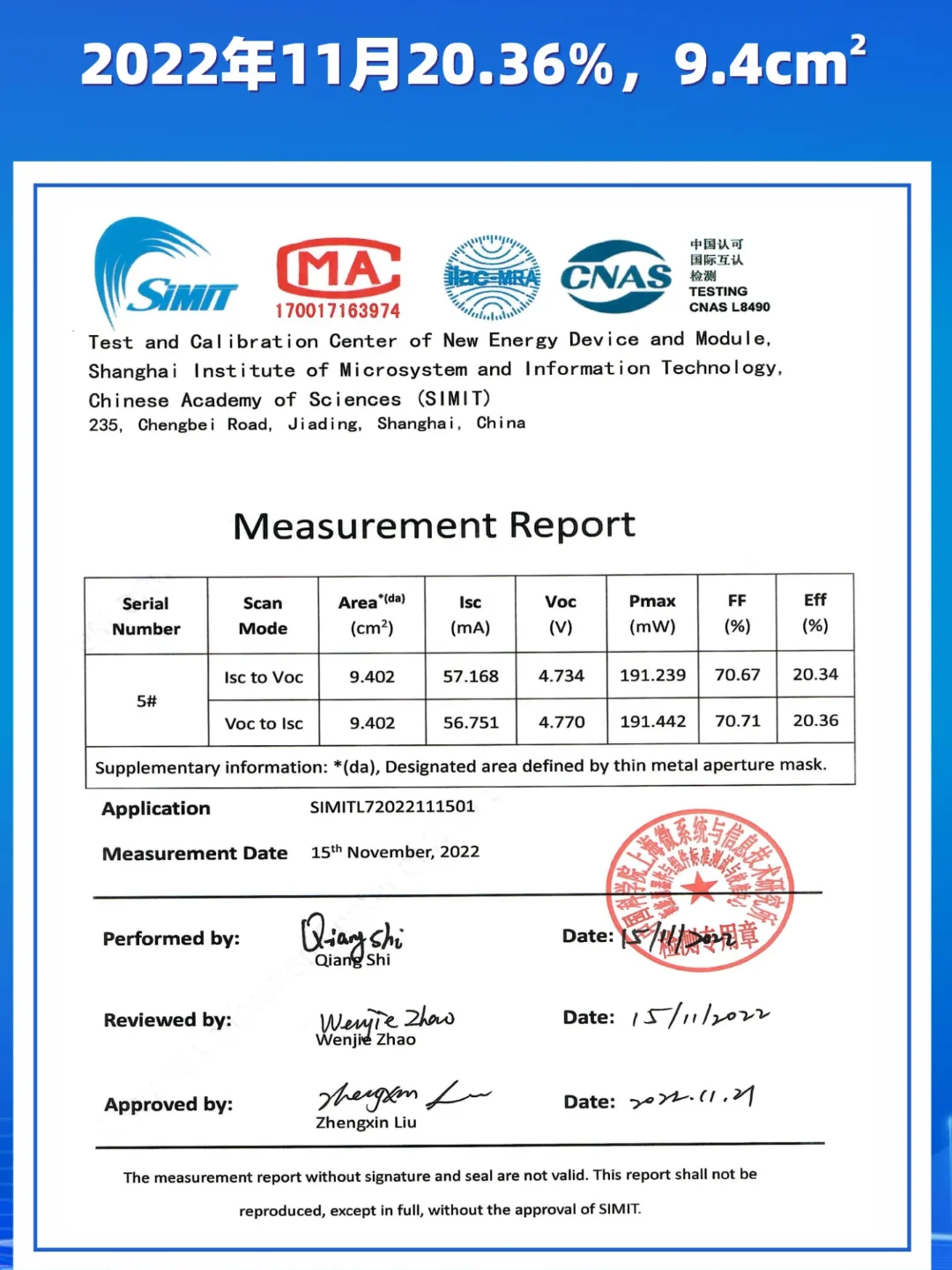
20.36%
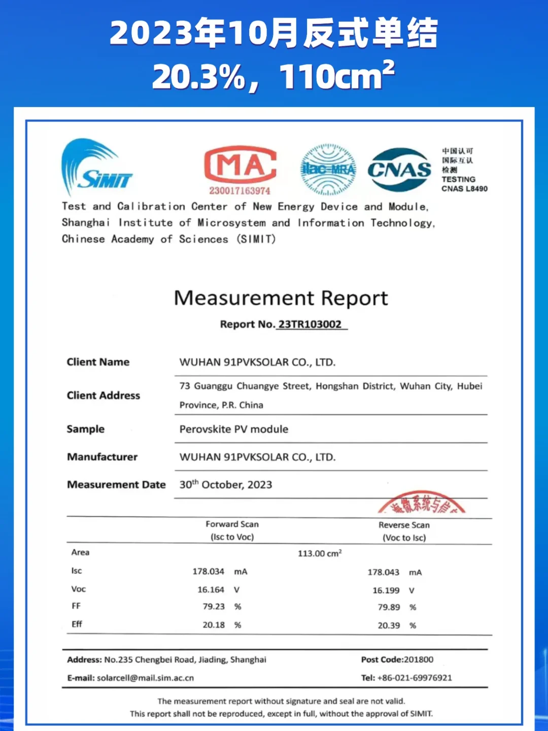
20.3%
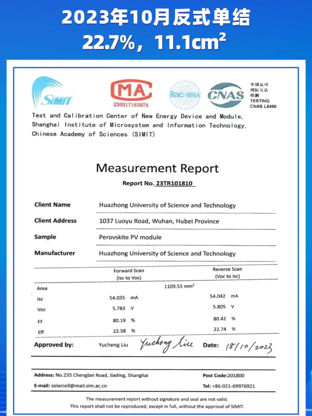
22.7%
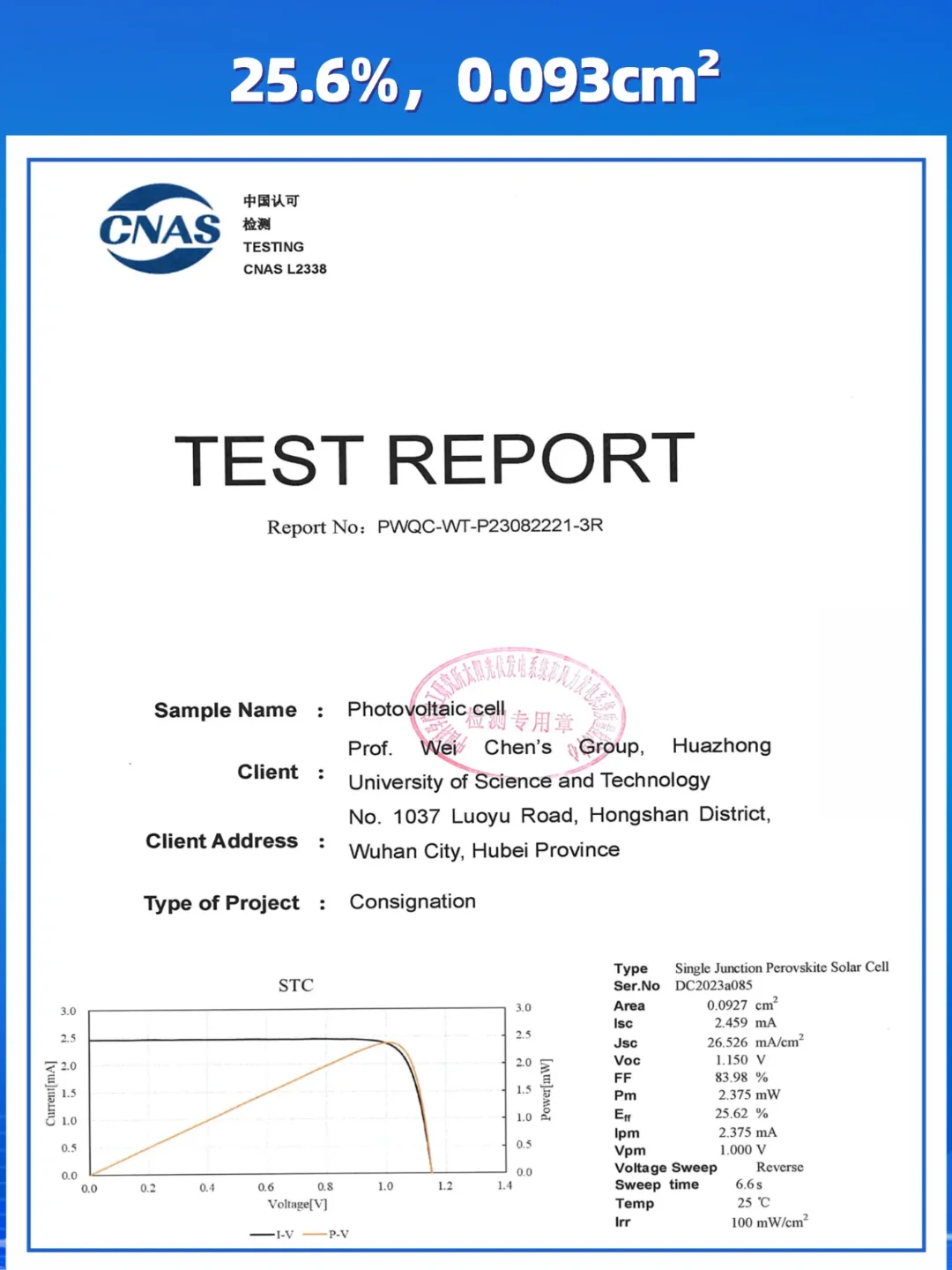
25.6%
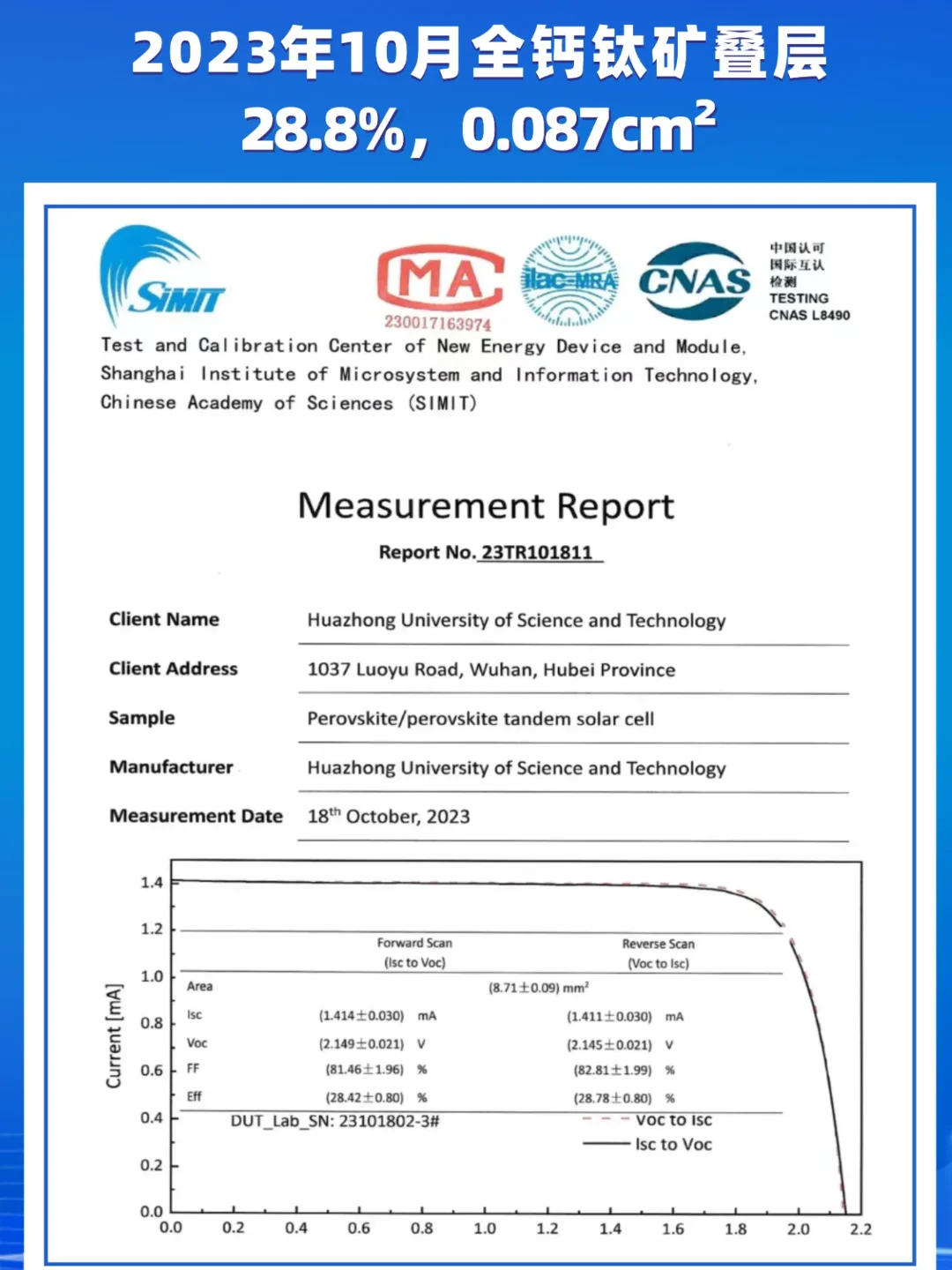
28.8%
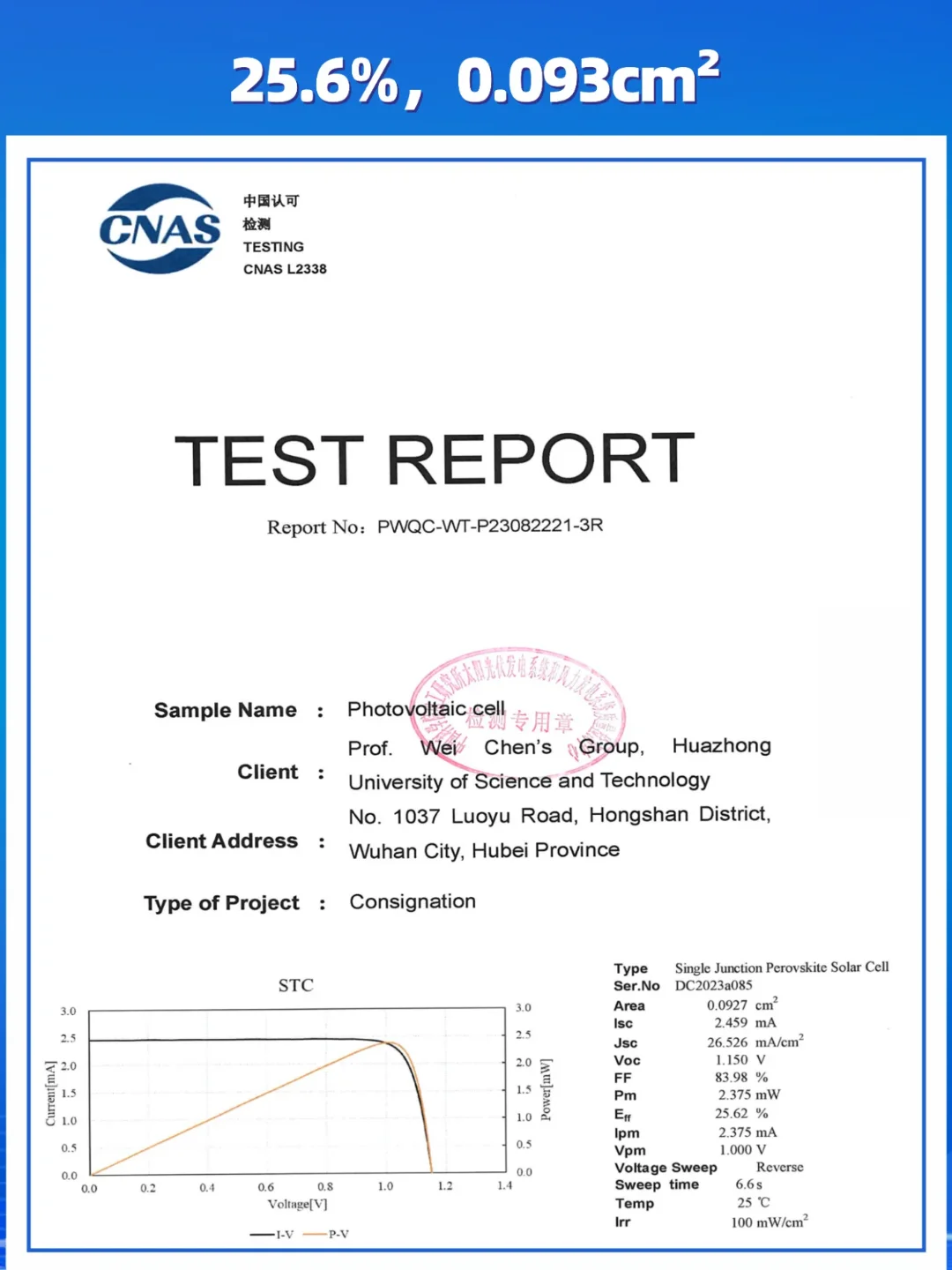
25.6%
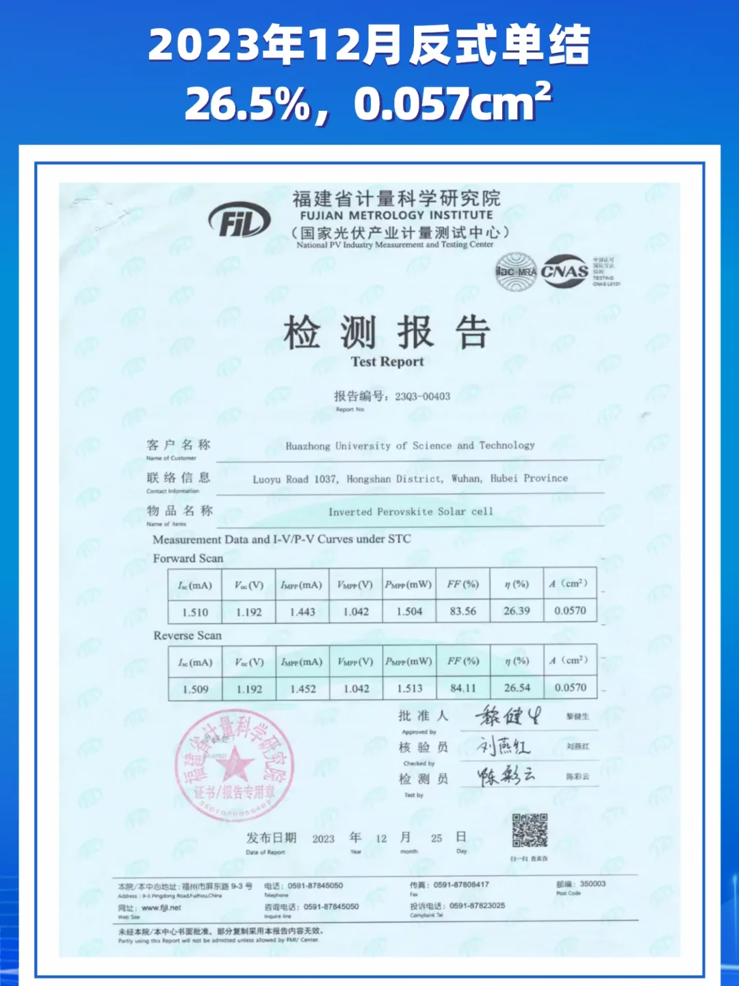
26.5%
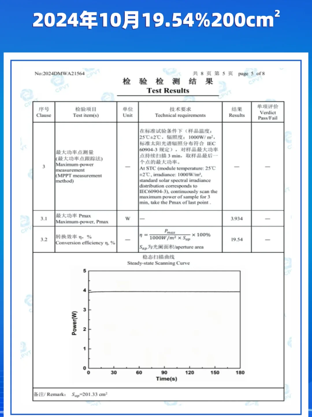
19.54%
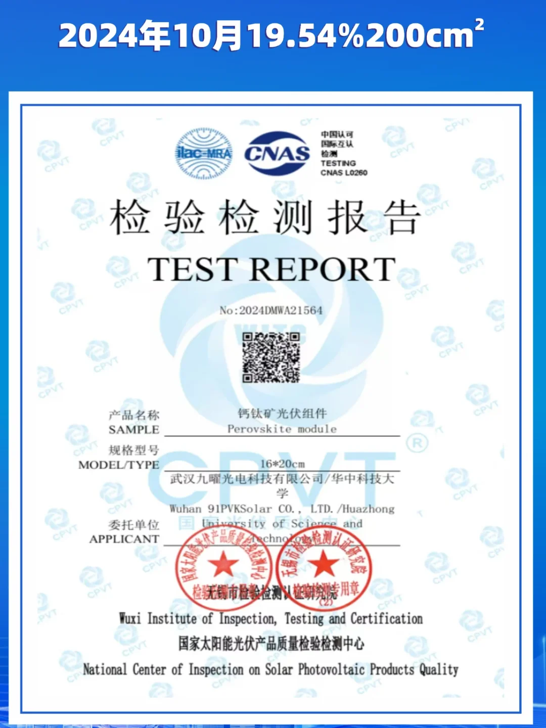
19.54%
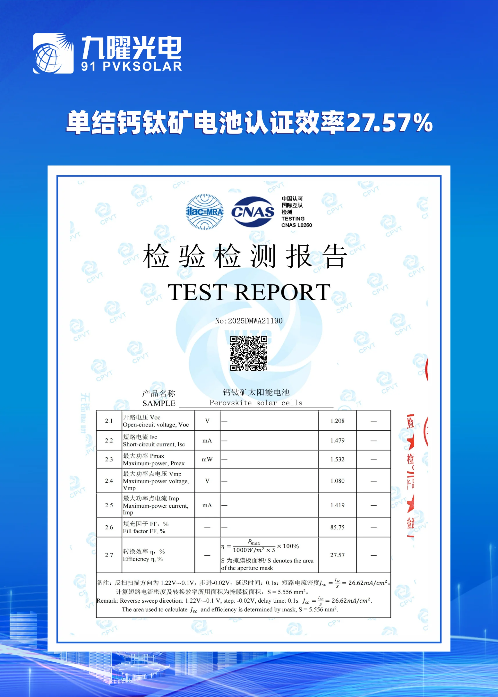
27.57%
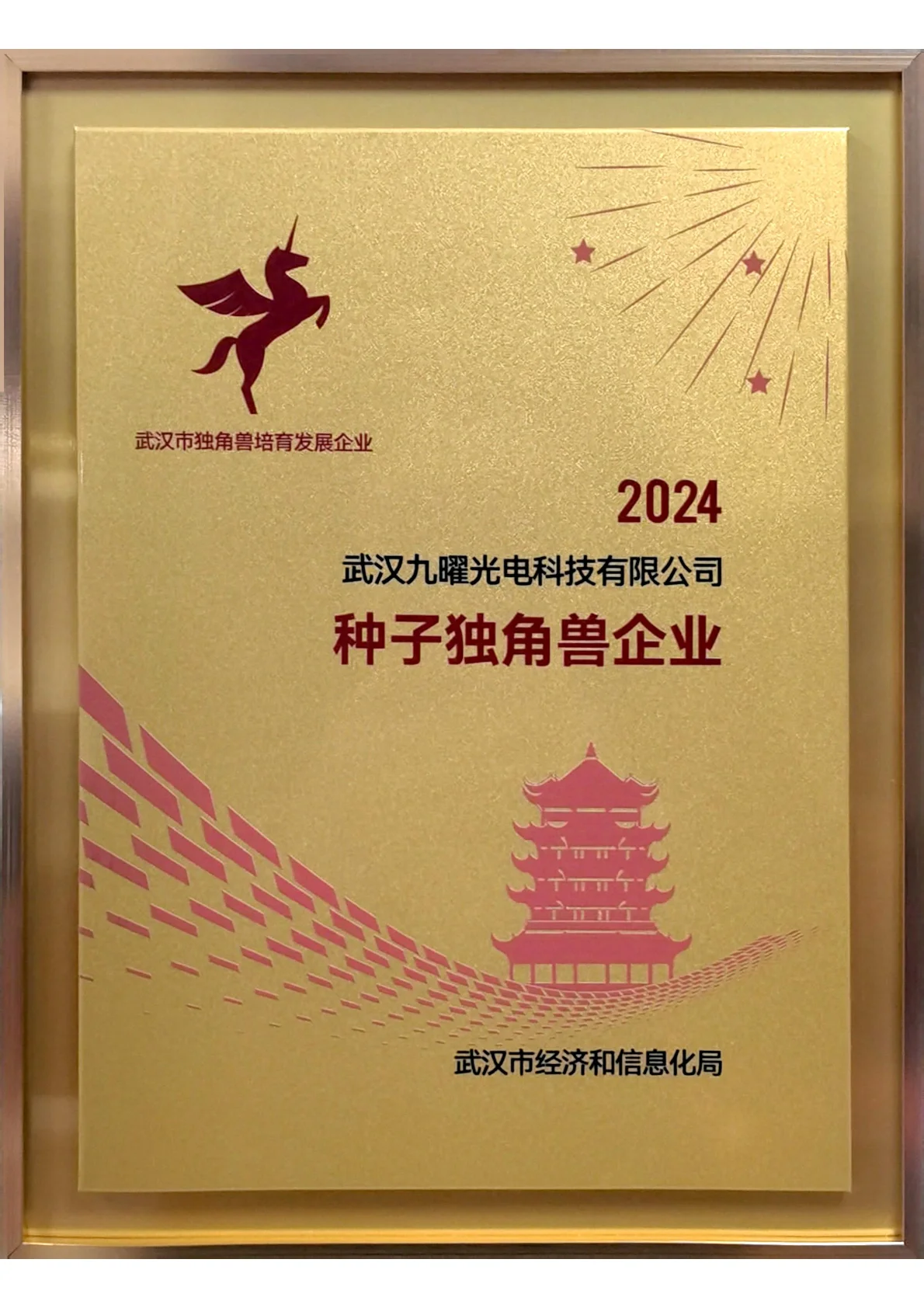
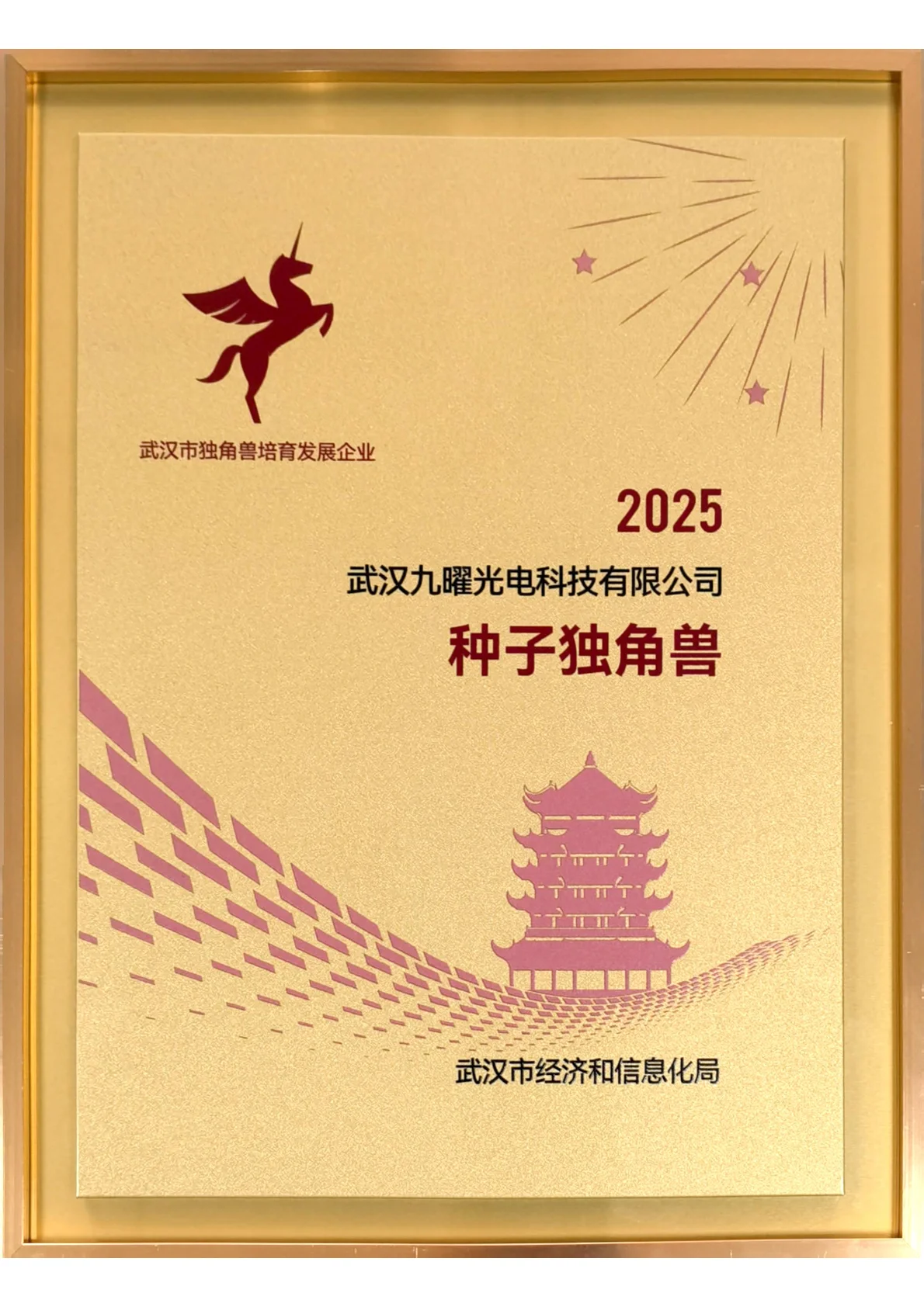
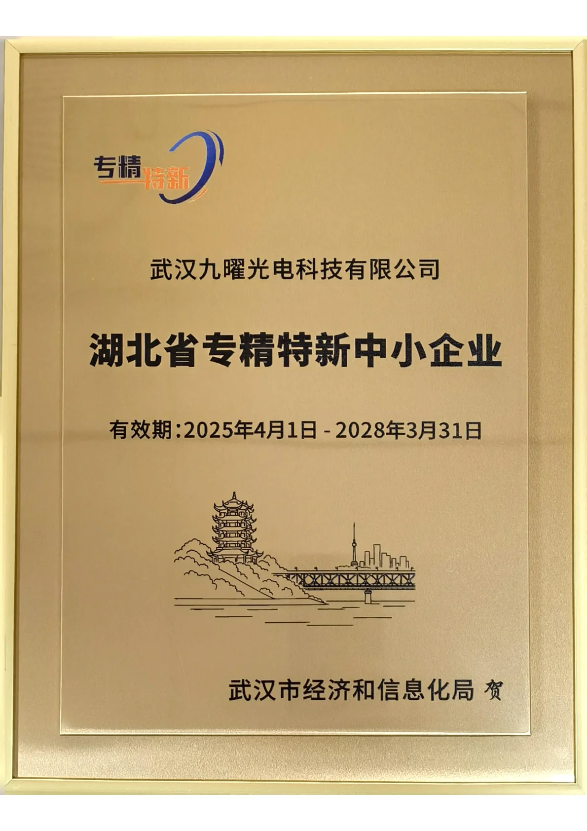
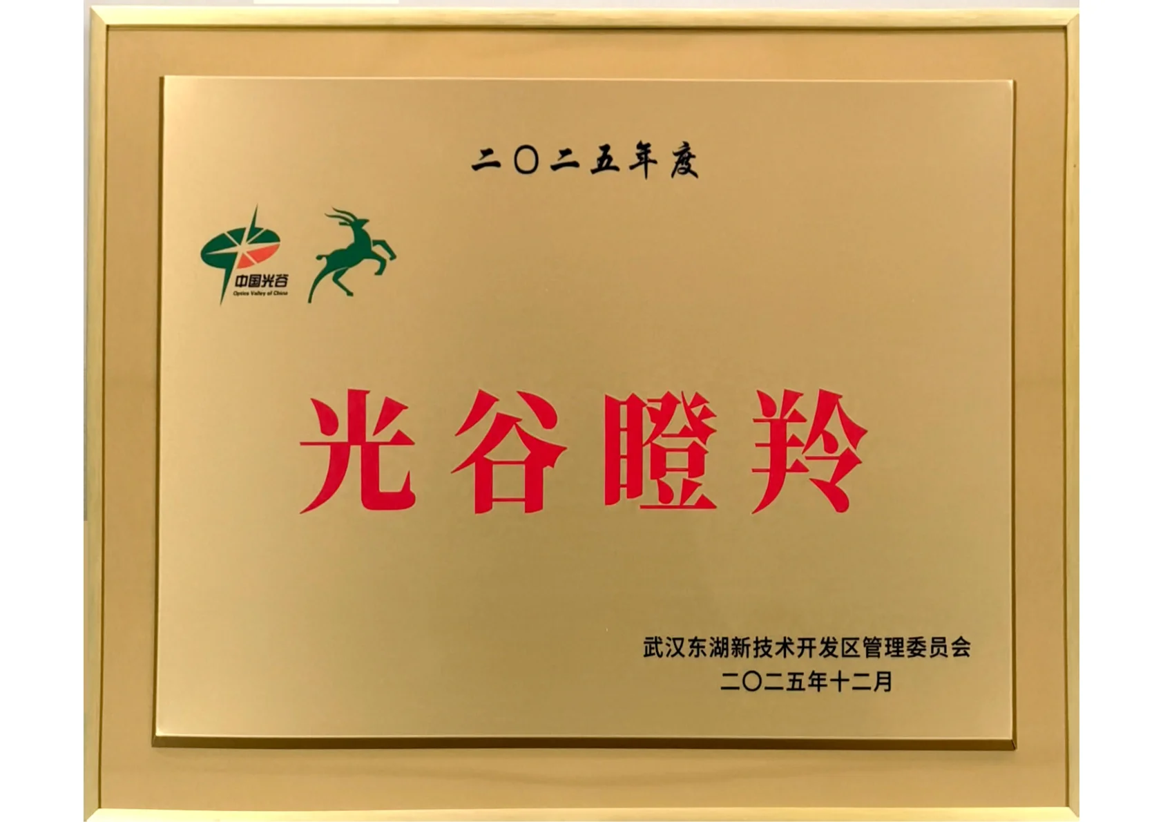
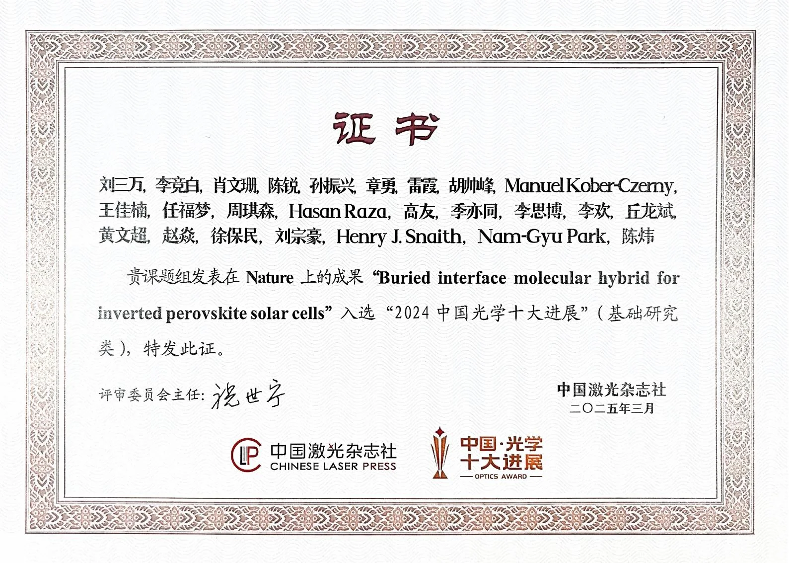
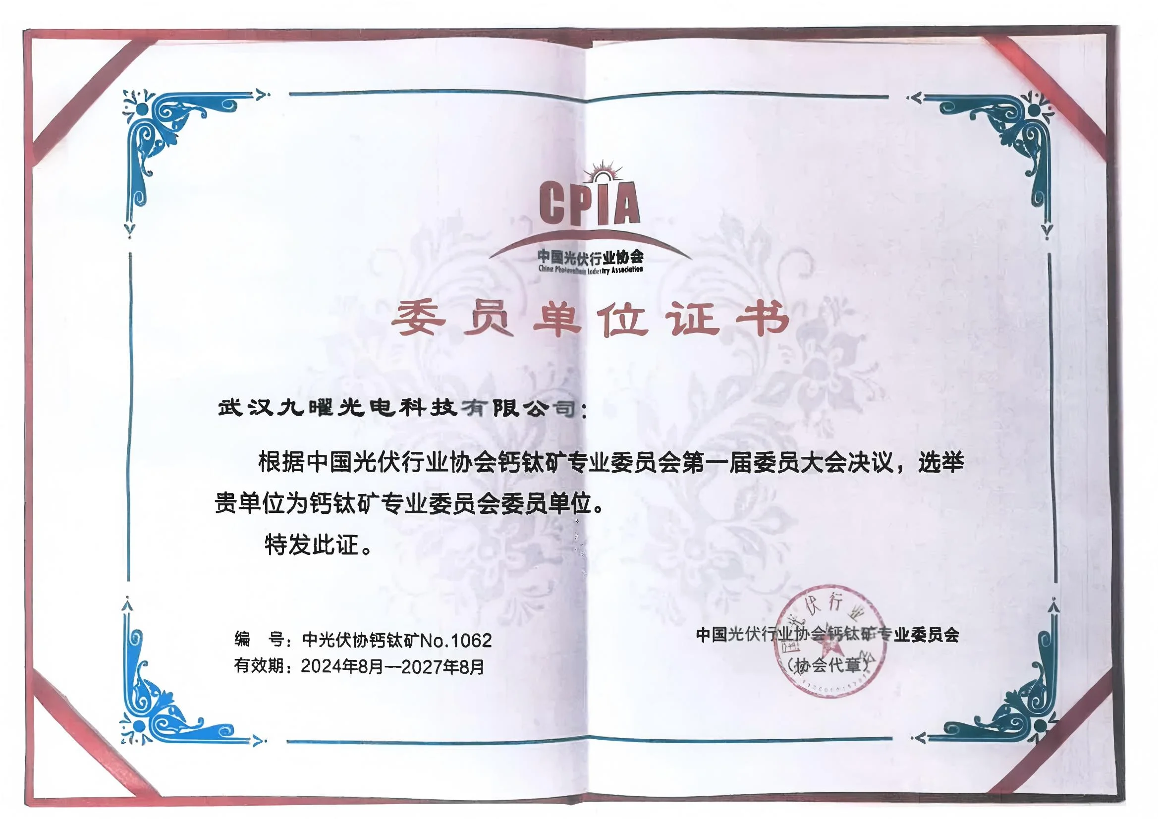
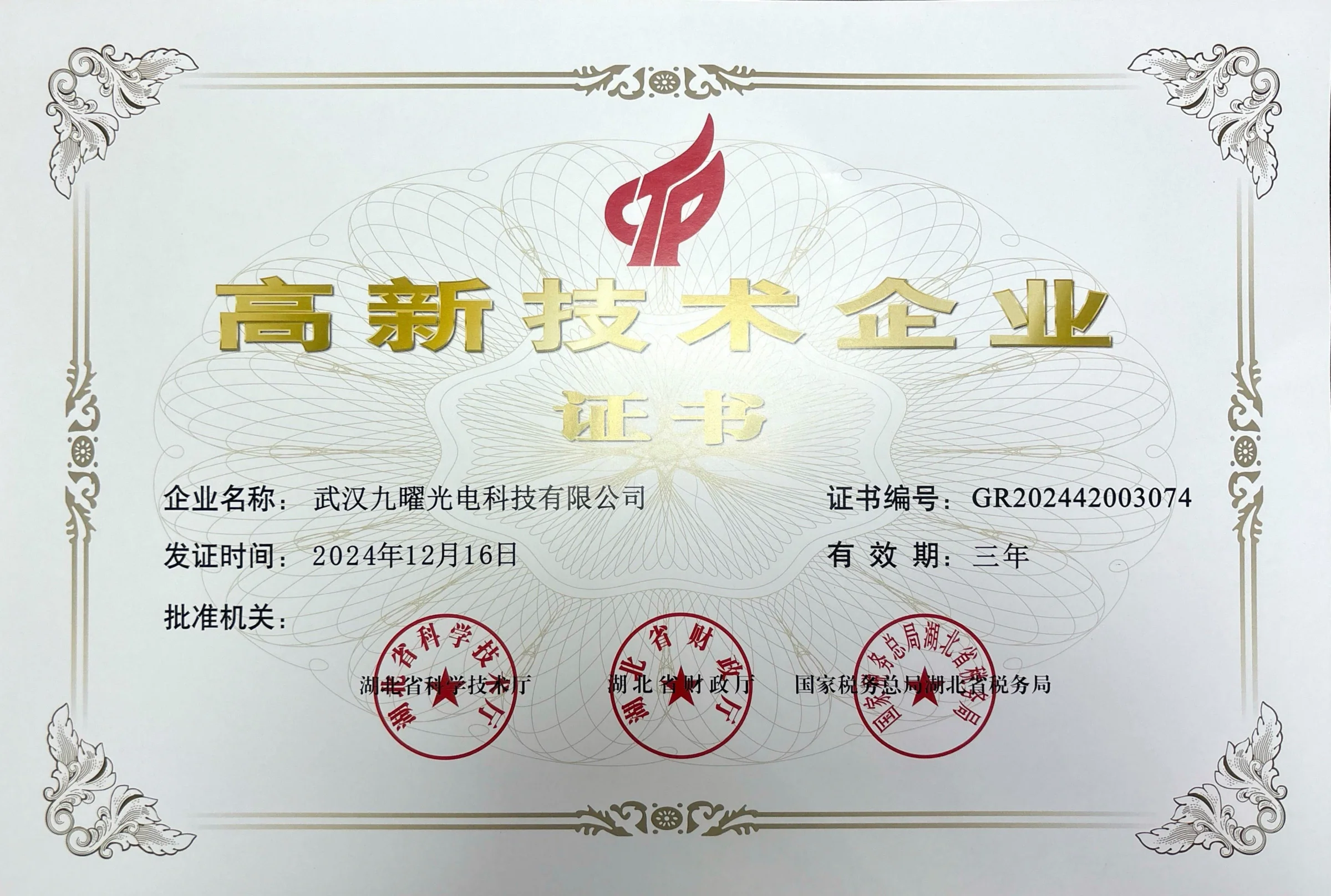
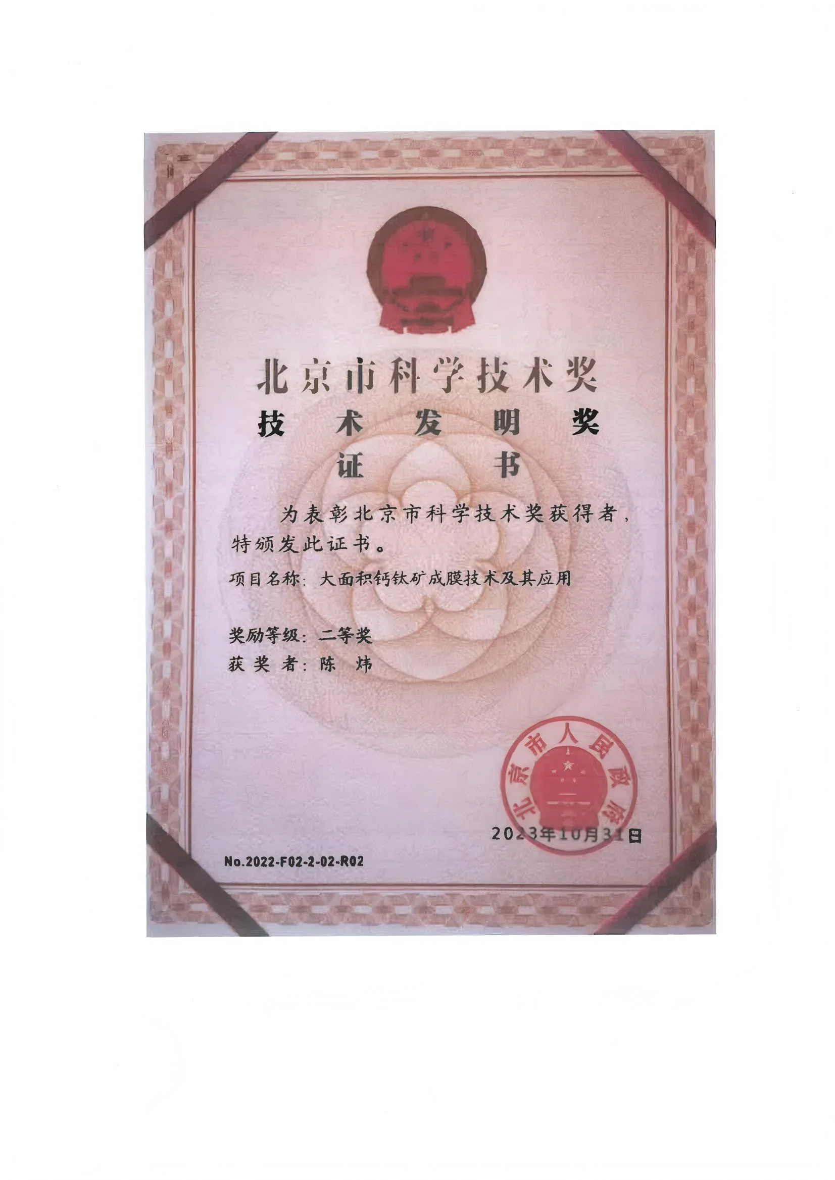
Honors
Process & Showcase Flow
Mass Production Process
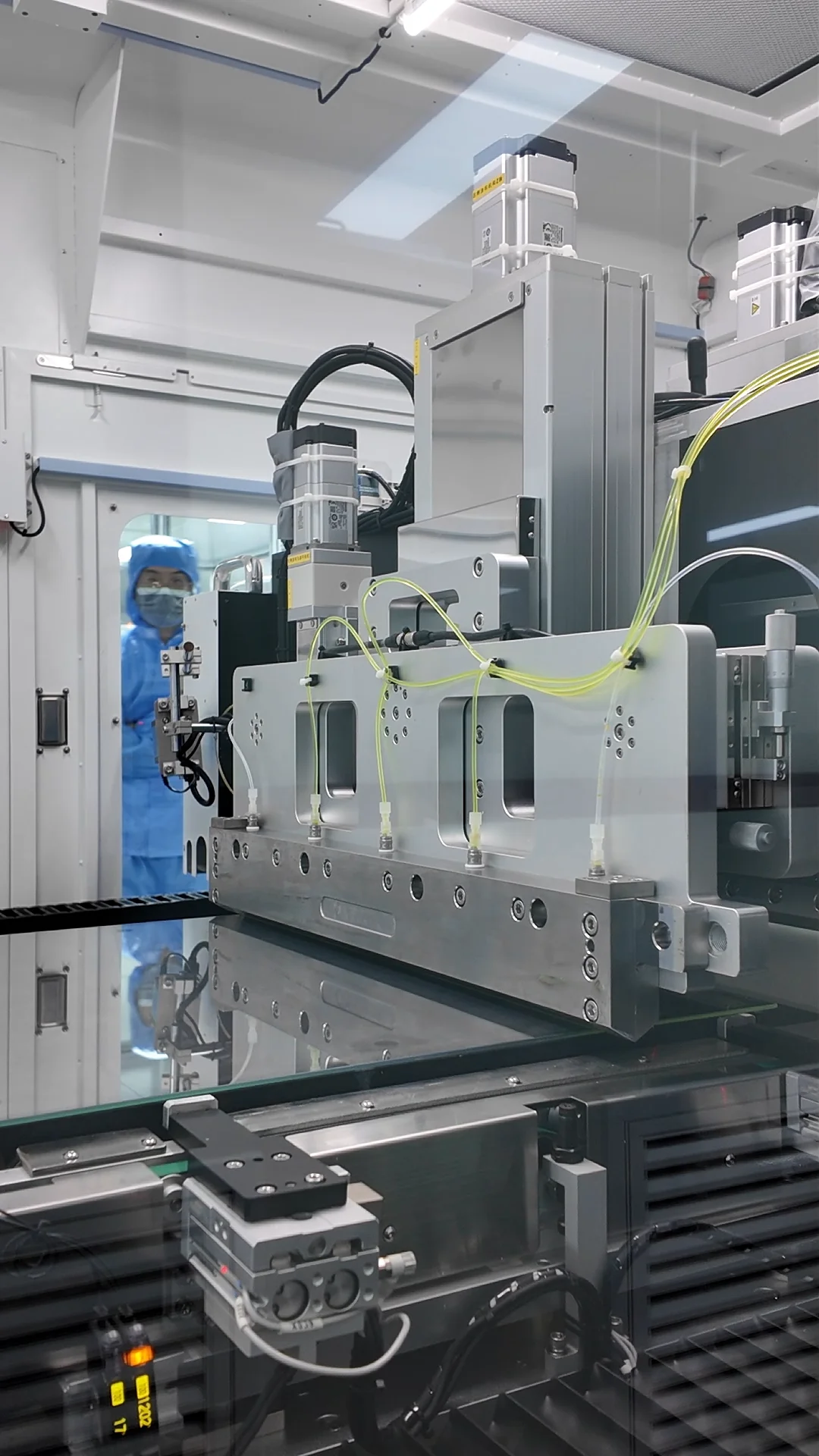
Slot-Die Coating
Slot-die coating moves perovskite modules from lab to GW-scale production. A precision die extrudes precursor solution through a micron-level gap for uniform large-area films, supporting rigid and flexible substrates with nanometer-level thickness control. Combined with in-situ crystallization control and an air knife, it eliminates edge effects and pinholes and keeps dead area below 3% in a 0.6m x 1.2m module, enabling high-yield, high-uniformity production at lower cost per watt.
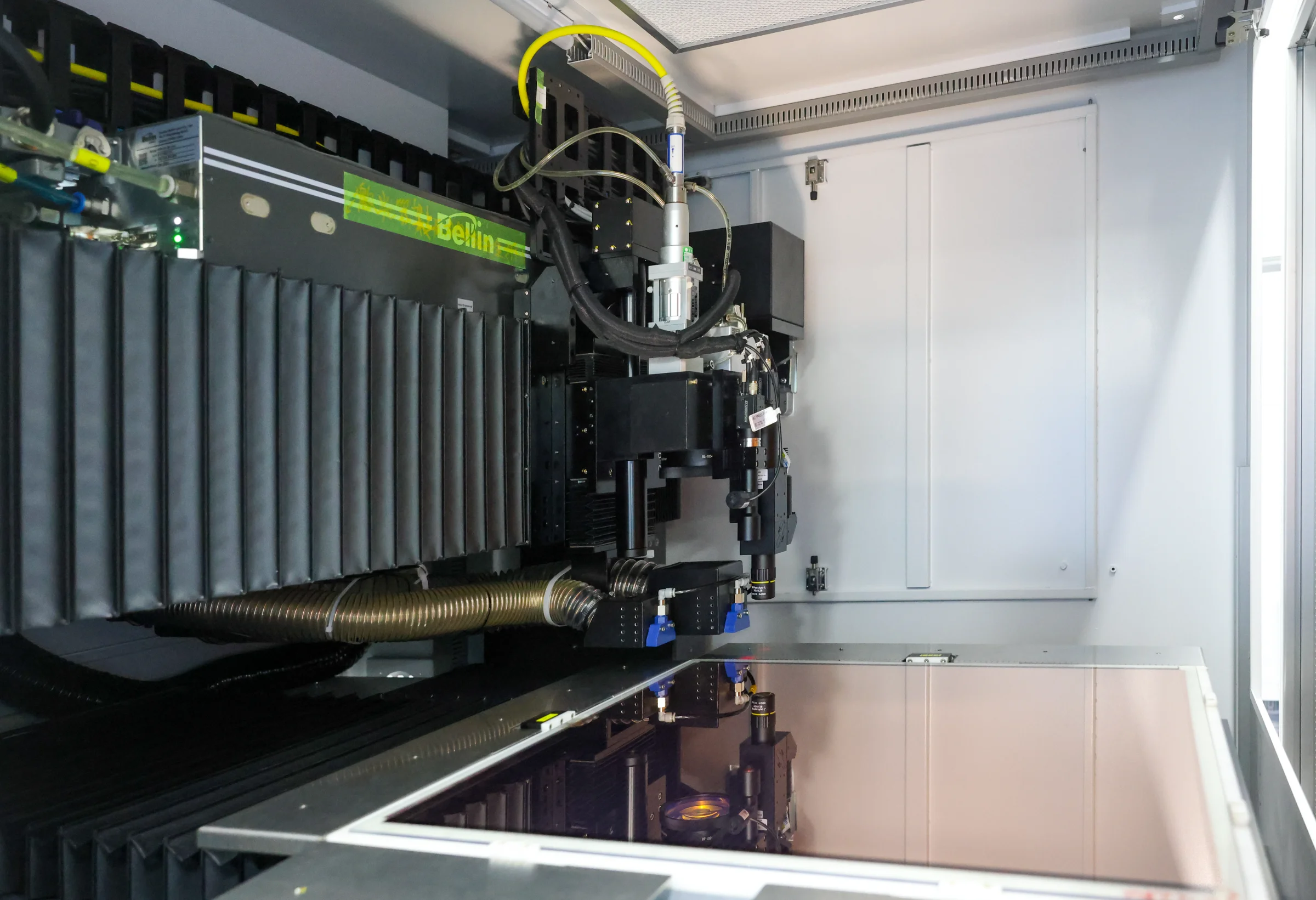
Laser Edge Cleaning
Laser edge cleaning
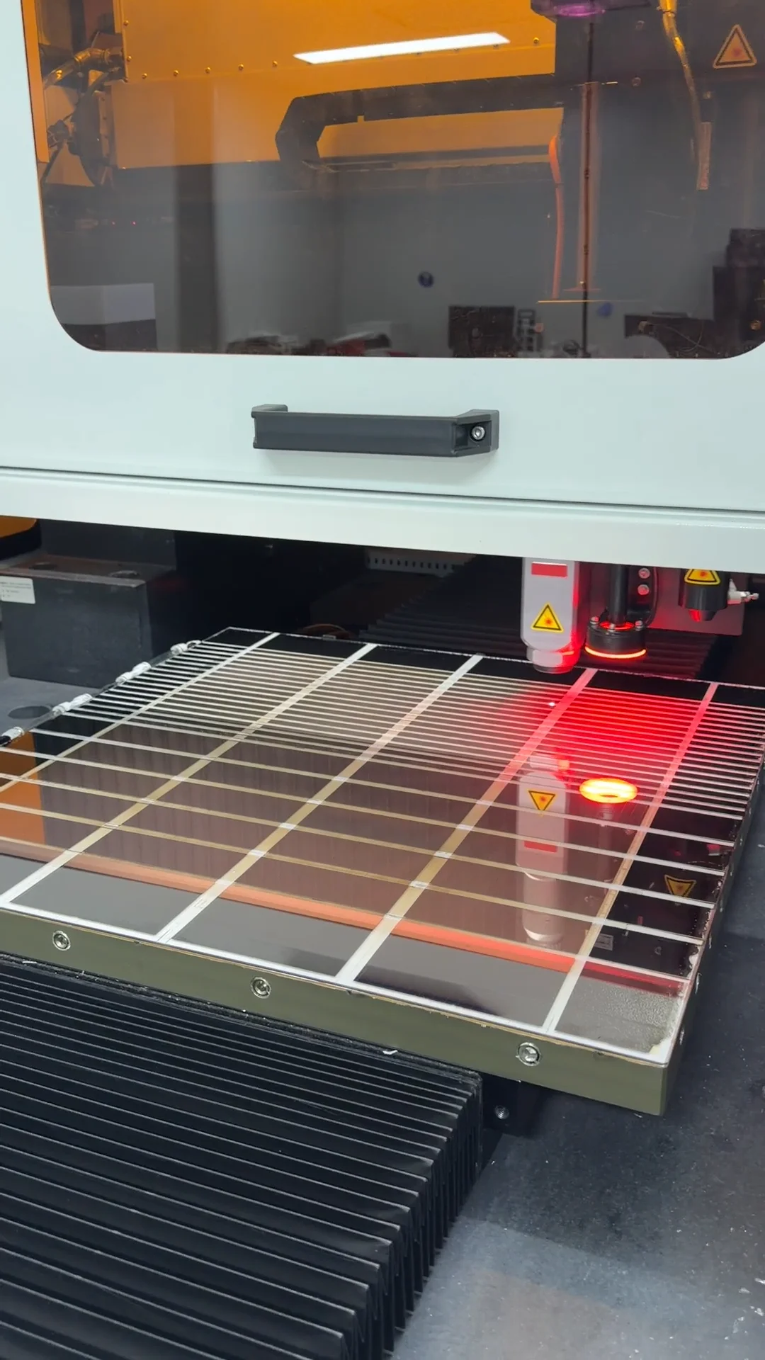
Laser Cutting
Laser cutting
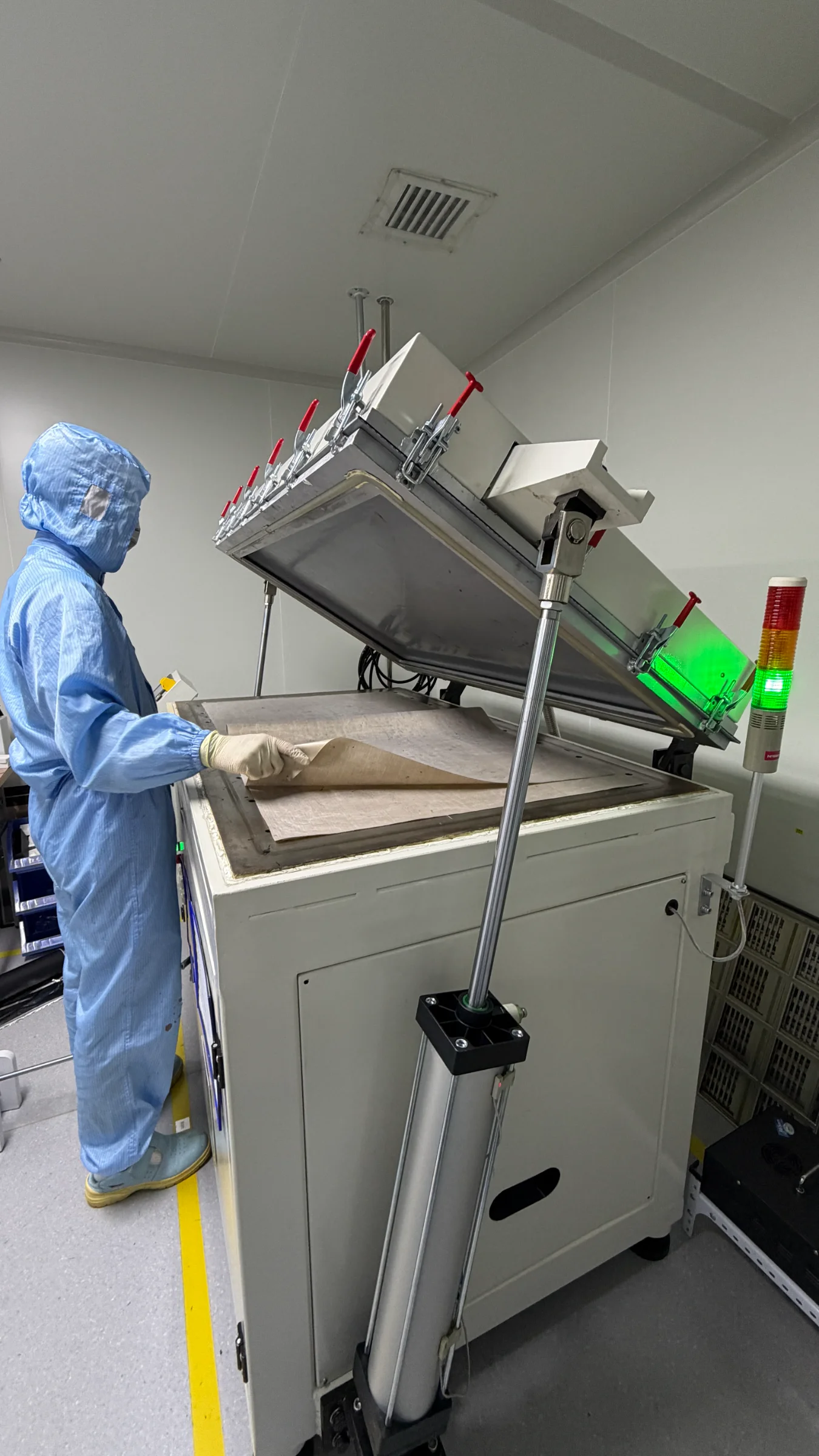
Lamination and Encapsulation
Lamination and encapsulation
Strict Quality Control
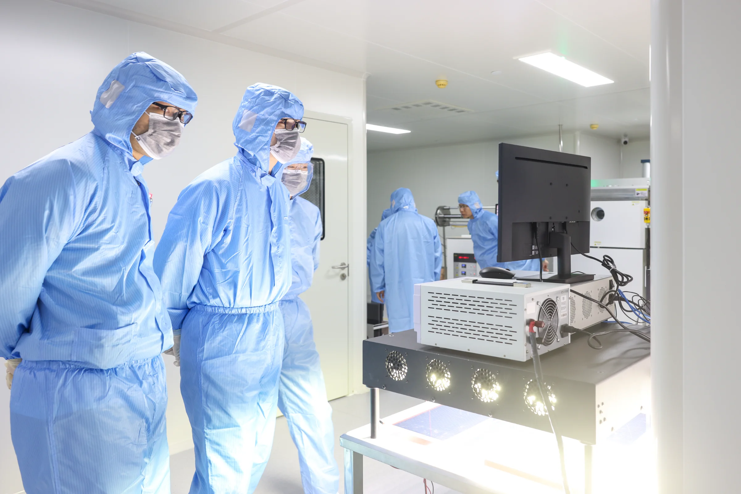
Automated Batch Efficiency Testing
Automated batch efficiency testing
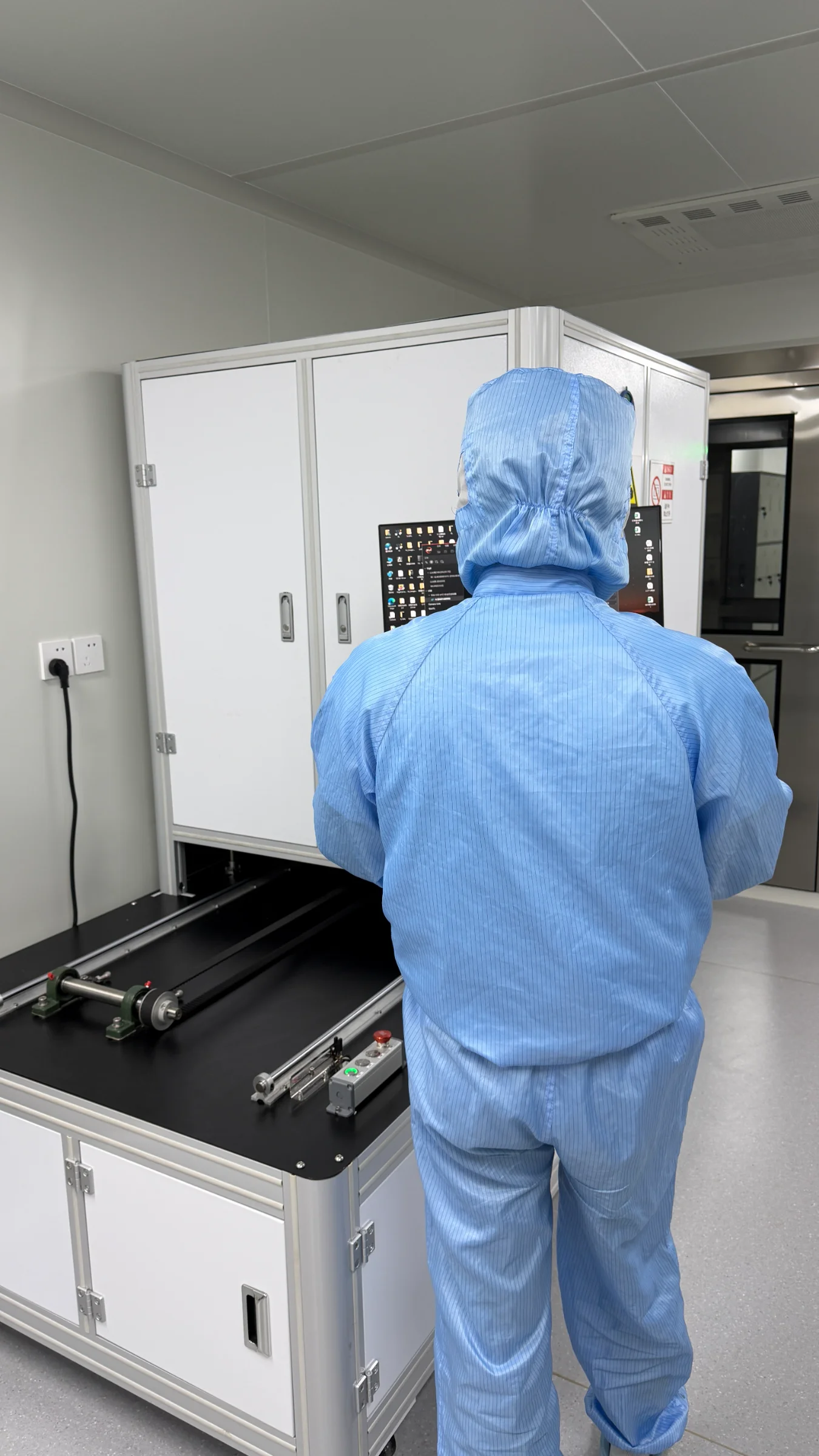
EL Inspection
EL inspection
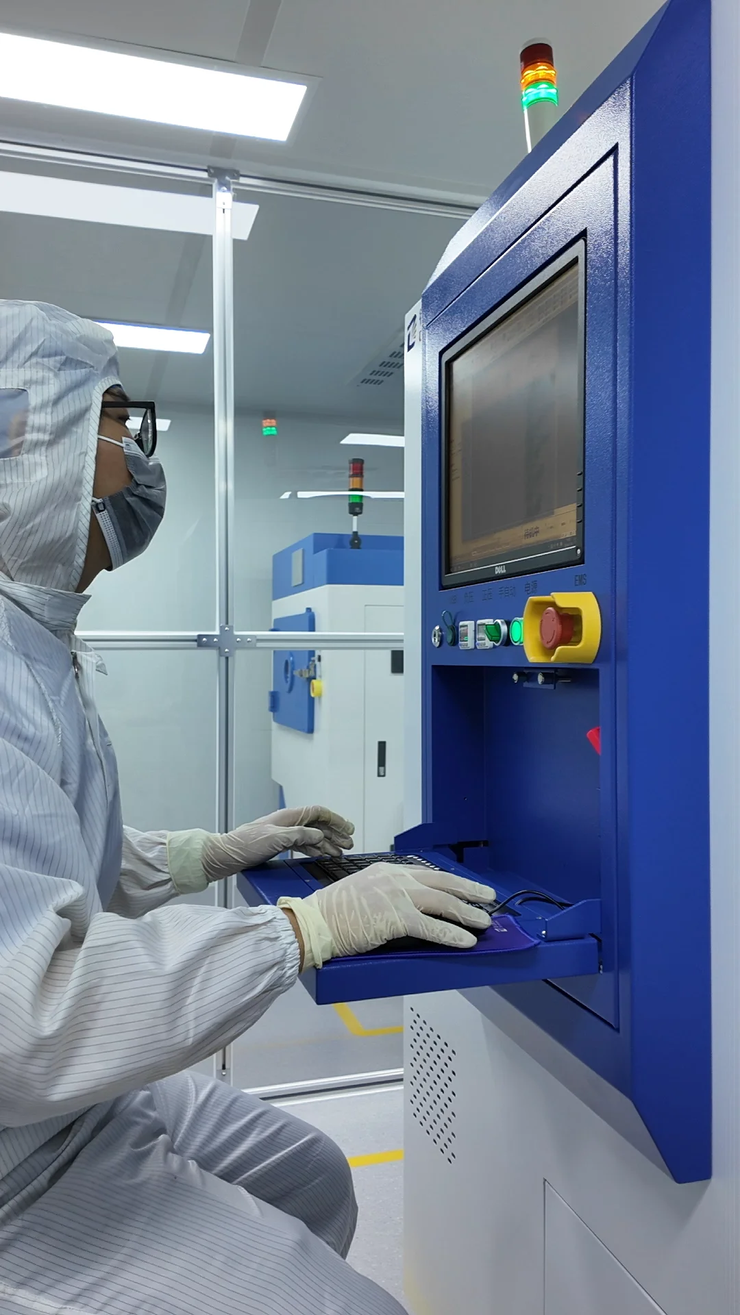
Visual Appearance Inspection
Visual appearance inspection
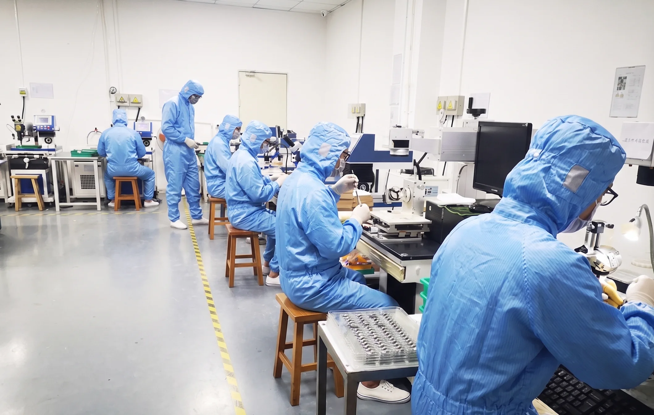
Automatic Marking and Batch Tracking
Automatic marking and batch tracking
Core Reliability Testing
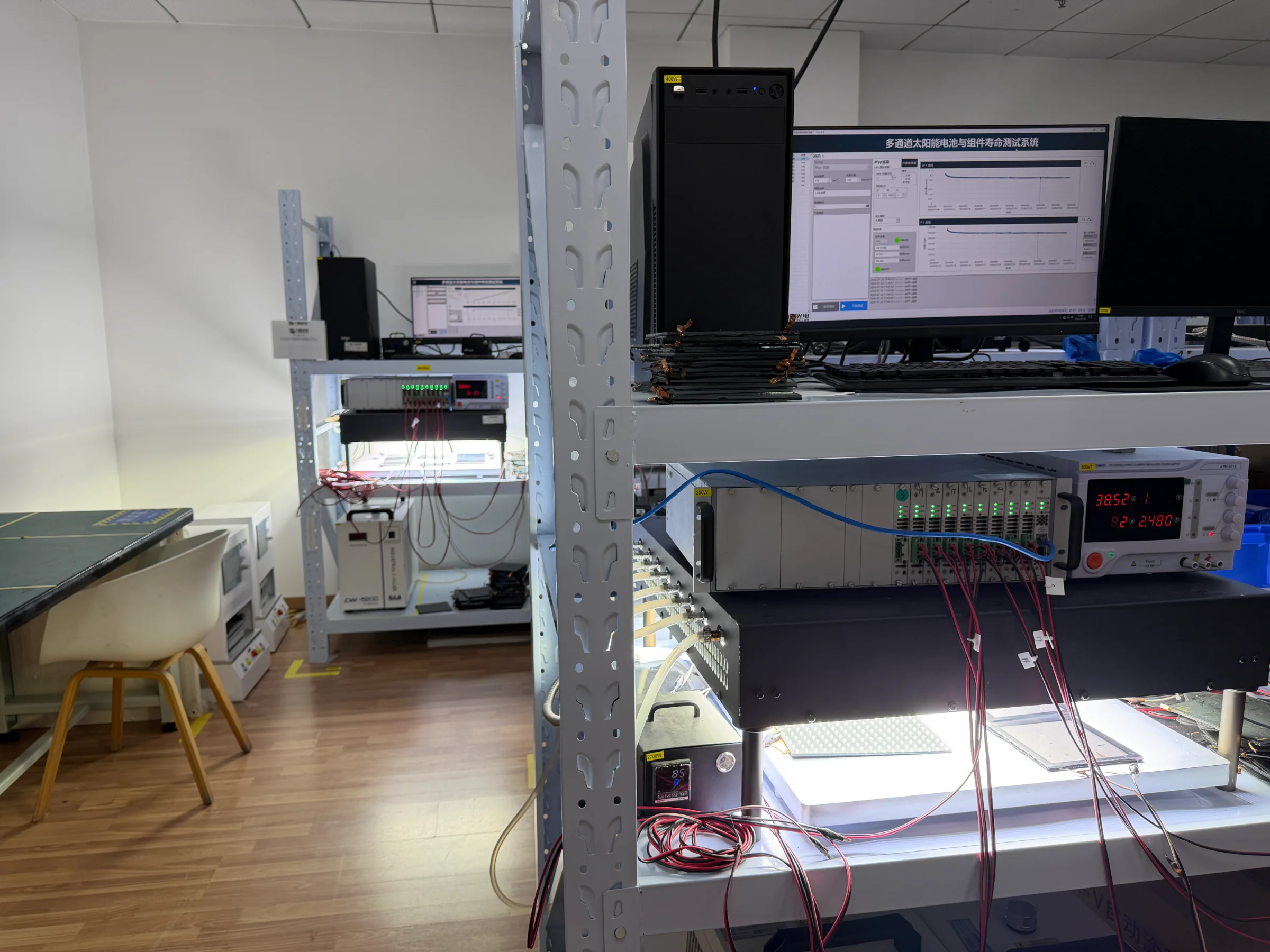
Light Aging at Different Temperatures
Light aging at different temperatures
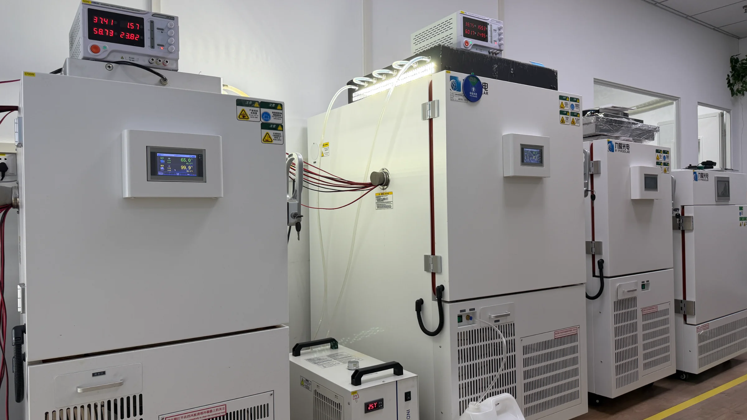
Damp Heat Aging
Damp heat aging
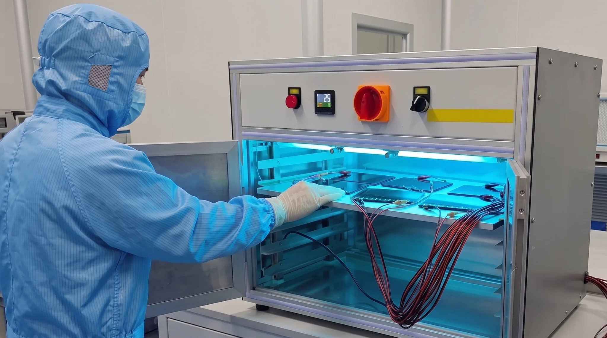
UV Aging
UV aging
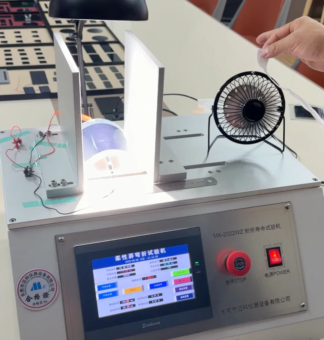
Flexible Bending Resistance Test
Flexible bending resistance test
Testing Capabilities
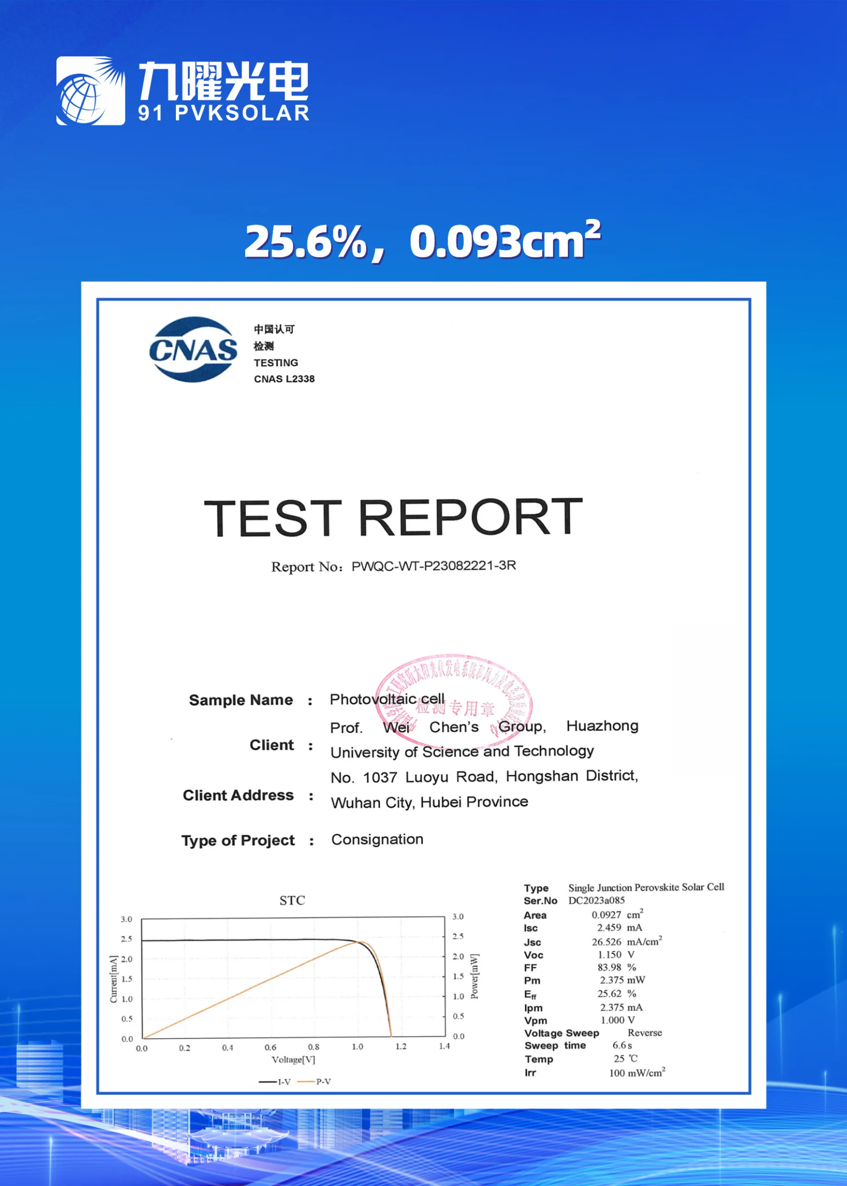
PID Degradation Test (Potential-Induced Degradation)
Contact Us
Address / Phone / Email